




Next EfficiencyUnlock in AI DatacenterInfrastructure
Traditional power stages in AI datacenter
System Power Flow Where
Power is Delivered and Lost
Facility infrastructure
(High Voltage)
- Utility Power Grid
- Substation & Transformer
- Primary UPS & Data Center
Server rack & board
(Intermediate Distribution)
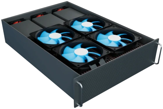
Power Distribution Unit
Compute package
(Point-of-Load Conversion)
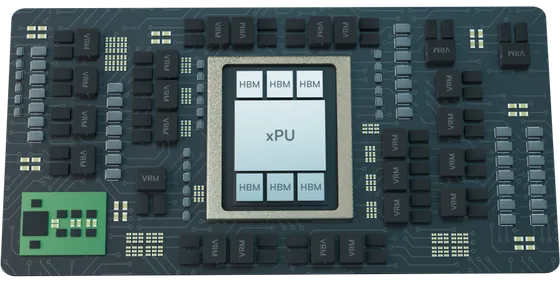

AI power wall from point-of-load voltage regulator
Lateral Power Delivery Limits GenAI Buildout
As xPU power scales, a growing share of total power is consumed by delivery overhead rather than compute.
0W
Total
0W
Total
0W
Total

The Problem
Power is lost before it
reaches compute
 IR drop across lateral traces in PCB and substrate.
 Voltage must be set higher to account for IR loss and droop.
01
Long electrical paths
Current crosses centimeters of board copper before it reaches the die.
02
Voltage drops under load
Transient compute spikes collapse the rail at the point of use.
03
Energy becomes wasted heat
Resistive loss along the path dissipates as thermal load.
Problem at scale
Wasted Power
Increases Non-Linearly
Conventional Motherboard Power Delivery
Example 1



Example 2













Architecture / Solution
Introducing the Monolithic Point-of-Load Chiplet

PowerMagix™ON-CHIP INDUCTOR

POWER FETs

Programmable Power Array (P²A™)CONTROLLER CIRCUITRIES


Powerlattice Point-of-Load IVR chiplet
First and Only Power
Chiplet in the Industry
Powerlattice chiplets
Vertically integrated under SoC package
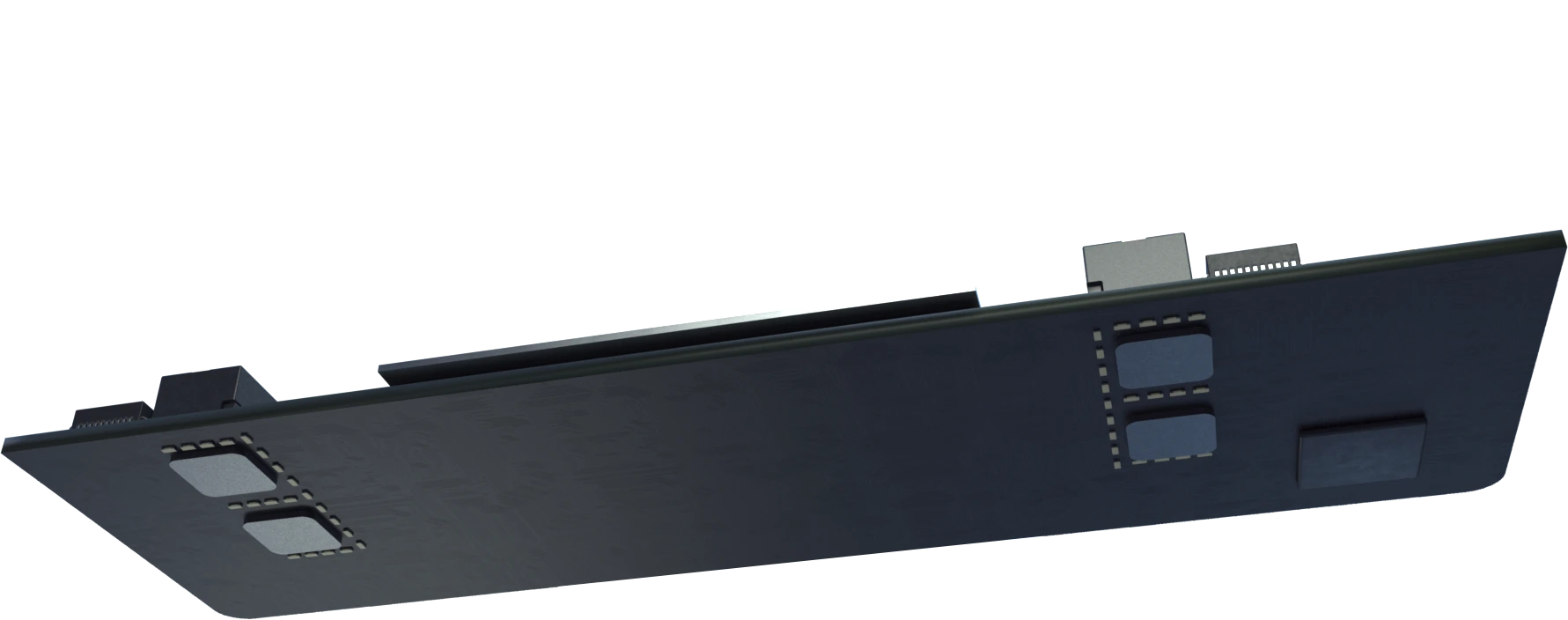
200X FASTER
ENABLES NEXT-GEN 3KW+ xPUS
> 400X DENSITY
xPU PACKAGE INTEGRATION
> 40%
POWER SAVINGS
How power is reduced
With IVR chiplet, SoC voltage can be set much lower
Powerlattice IVR Eliminates Over-provisioned Guard Band in Supply Voltage
- On-die supply voltage from the existing power solution
- On-die supply voltage from Powerlattice IVR
Impact
0%
Lower power
with Powerlattice IVR chiplet